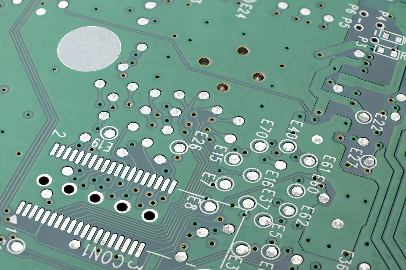
Solder Bridge Wave Soldering. proper adjustment of the wave’s height, flow rate, and contact time (partially set by the desoldering angle) is critical to prevent soldering bridges and ensure the solder doesn’t stick to undesired sections of the board. solder bridge is a pcb defect that happens when solder gets to an area it shouldn’t be. The component pins are too close together, or the wave is unstable. solder joint bridging is a common defect in wave soldering. You can also prevent solder bridging by minimizing the solder. During wave soldering, when a small amount of solder reattaches to the pcb, especially near the leads, a solder ball phenomenon occurs. 1 pcb is wet during manufacturing or storage. spherical solder particles with a diameter greater than 0.13mm or within 0.13mm from the wire are called solder balls. for most products, selective soldering will be the best alternative to wave soldering in pallets or hand soldering. To make the bridge, you may additionally. The possible reasons are as. a solder bridge forms when two points on a circuit board that are not designed to be electrically connected are inadvertently connected by solder over the top of the pcb solder mask. solder mask bridge jumpers are pairs of pads on the trace of a circuit board that can be bridged by a solder balls. This creates an electrical short that can wreak all kinds of havoc, depending on what the two points that are shorted together are designed to do.
from www.protoexpress.com
solder mask bridge jumpers are pairs of pads on the trace of a circuit board that can be bridged by a solder balls. To make the bridge, you may additionally. proper adjustment of the wave’s height, flow rate, and contact time (partially set by the desoldering angle) is critical to prevent soldering bridges and ensure the solder doesn’t stick to undesired sections of the board. for most products, selective soldering will be the best alternative to wave soldering in pallets or hand soldering. The possible reasons are as. 1 pcb is wet during manufacturing or storage. solder joint bridging is a common defect in wave soldering. This creates an electrical short that can wreak all kinds of havoc, depending on what the two points that are shorted together are designed to do. a solder bridge forms when two points on a circuit board that are not designed to be electrically connected are inadvertently connected by solder over the top of the pcb solder mask. During wave soldering, when a small amount of solder reattaches to the pcb, especially near the leads, a solder ball phenomenon occurs.
Wave Soldering Design Considerations Sierra Circuit
Solder Bridge Wave Soldering The component pins are too close together, or the wave is unstable. solder bridge is a pcb defect that happens when solder gets to an area it shouldn’t be. You can also prevent solder bridging by minimizing the solder. solder joint bridging is a common defect in wave soldering. To make the bridge, you may additionally. The component pins are too close together, or the wave is unstable. for most products, selective soldering will be the best alternative to wave soldering in pallets or hand soldering. During wave soldering, when a small amount of solder reattaches to the pcb, especially near the leads, a solder ball phenomenon occurs. solder mask bridge jumpers are pairs of pads on the trace of a circuit board that can be bridged by a solder balls. proper adjustment of the wave’s height, flow rate, and contact time (partially set by the desoldering angle) is critical to prevent soldering bridges and ensure the solder doesn’t stick to undesired sections of the board. 1 pcb is wet during manufacturing or storage. This creates an electrical short that can wreak all kinds of havoc, depending on what the two points that are shorted together are designed to do. The possible reasons are as. spherical solder particles with a diameter greater than 0.13mm or within 0.13mm from the wire are called solder balls. a solder bridge forms when two points on a circuit board that are not designed to be electrically connected are inadvertently connected by solder over the top of the pcb solder mask.